Table of Contents
CPU - DSP1C
TODO
- try dump with JTAG (could be found by brute-force)
Basic description
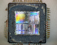
Custom chip (ASIC) made for Vaisala by VLSI solution.
signature:
DSP1C
VAISALA
1101C
37130
Chip manufacturing process is 3 layer metal.
Pinouts
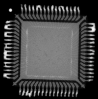
Pins are numbered counterclock-wise, pin 1 is near the small pit (ignore possible 2 large circles placed orthogonaly).
Pin state has been measured with osciloscope. Timing informations are inoccurate (+-50%).
| PIN No. | state (type) | description |
|---|---|---|
| 1 | GND | |
| 2 | VCC | |
| 3 | I_SIGN (in) | noise - signal from GPS RF module |
| 4 | I_MAGN (in) | noise - signal from GPS RF module |
| 5 | Q_SIGN (in) | noise - signal from GPS RF module |
| 6 | Q_MAGN (in) | noise - signal from GPS RF module |
| 7 | CLK (in) | 16.3676 MHz - clock from GPS RF module |
| 8 | 0 | |
| 9 | 0 | |
| 10 | 0 | |
| 11 | 0 | |
| 12 | 0 | |
| 13 | GND | |
| 14 | VCC | |
| 15 | POW_RESET_IN (in) | Power on reset |
| 16 | POW_RESET_OUT (out) | go from 0 to 1 approx. 2 ms after powering CPU |
| - | - | - |
| 17 | SPI CLK | |
| 18 | SPI MISO | |
| 19 | SPI MOSI | |
| 20 | SPI /CS EEPROM | |
| 21 | 1, ? /CS ? CON5 pin 10 | |
| 22 | SPI /CS GPS, IC3 - pin 18 | |
| 23 | 1 | |
| 24 | GND | |
| 25 | VCC | |
| 26 | 1 | |
| 27 | 1 | |
| 28 | CLK (250 μs), CON5 pin 2 | |
| 29 | DATA (400 μs), CON5 pin 3 | |
| 30 | 0 | |
| 31 | 1 | |
| 32 | 0 | |
| - | - | - |
| 33 | GND | |
| 34 | VCC | |
| 35 | CLK (50 μs) | |
| 36 | connected to GND | |
| 37 | connected to GND | |
| 38 | connected to GND | |
| 39 | 1 | |
| 40 | connected to GND | |
| 41 | CLK (1 μs) | |
| 42 | connected to GND | |
| 43 | DATA (150 ns) | |
| 44 | GPIO_1_15 | 0 |
| 45 | GPIO_1_14 ? | 0 |
| 46 | GPIO_1_13 ? | 1 |
| 47 | GND | |
| 48 | VCC | |
| - | - | - |
| 49 | GPIO_1_12 | 1, CON5 - pin 4 |
| 50 | GPIO_1_11 | 0, CON5 - pin 11 |
| 51 | GPIO_1_10 | 0, CON5 - pin 12 |
| 52 | GPIO_1_9 | 1, CON2 - pin6 |
| 53 | GPIO_1_8 | 1 |
| 54 | GPIO_1_7 | 1, CON6 - pin 7, ? heating, 0 = on, 1 = off |
| 55 | GPIO_1_6 | 0, CON6 - pin 8, ? select heated element, 0 = upper, 1 = lower |
| 56 | GPIO_1_5 | 0, CON6 - pin 2, ? |
| 57 | GND | |
| 58 | VCC | |
| 59 | GPIO_1_4? | 1 |
| 60 | GPIO_1_3? | 1 |
| 61 | GND | |
| 62 | GPIO_1_2? | 1, CON2 - pin 1 |
| 63 | GPIO_1_1 | 0 |
| 64 | GPIO_1_0 | 0 |
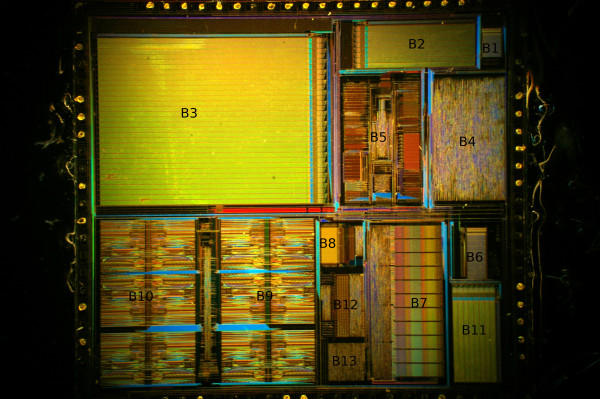
CPU building blocks
| block name | type | description |
|---|---|---|
| B1 | ROM (2KB) | 1K x 16 bit, mapped to Y, offset 0x1000 |
| B2 | SRAM (4KB) | 256 x 16 x 8 bits, mapped to Y, offset 0x0 |
| B3 | SRAM (32KB) | 512 x 32 x 16 bits, used for code, mapped to X, offset 0x2000 |
| B4 | ??? | something relly complicated |
| B5 | ??? | block made from few smaller blocks |
| B6 | ROM (4KB) | 32 bit bus, code (bootloader and some basic routines), mapping to address space not found (anny way to read it by software?) |
| B7 | ??? | looks like long and a bit entangled wires |
| B8 | memory/registers? | ??? |
| B9, B10 | GPS | 12x GPS processing block |
| B11 | SRAM (3KB) | 192 x 16 x 8 bits, mapped to X, offset 0x0 |
| B12 | ??? | something with more stages |
| B13 | ??? | something complicated |
Those units might be implemented in HW:
- CRC16
- Reed-Solomon (result is 24B long)
- some GPS related stuff
- instruction decoder
CPU peripherals (SPI/GPIO/...)
I/O mapping
BUS X
| address(es) | boot value | description |
|---|---|---|
| 0x0000 - 0x05FF | - | X-RAM |
| 0x2000 - 0x6000 | - | ???, instruction memory I/O port |
| 0xFF83, 0xFF85 | ??? | ??? FW - (0xff83) = 0x3c3c, (0xff85) = 0x2d2d |
| 0xFF95 | ??? | FW, → A0 |
| 0xFF96 | 0xffbf | ??? |
| 0xFF97 - 0xFF98 | 0xffff, 0xffff | ??? |
| 0xFF99 | 0xfdff | ???, constant |
| 0xFFA0 | 0x4000 | ???, settable bits: 0xffc3, … |
| 0xFFA1, 0xFFA2 | ??? | ???, FW: read to A as pair (0xFFA1, 0xFFA2) → (A0, A1) |
| 0xFFA4 | 0x0001 | SPI_CONFIG, settable bits: 0x01f7, … |
| 0xFFA5 | 0x0001 | SPI_DATA, read recieved data, (write to send data?) |
| 0xFFA6 | 0x0000 | SPI, EEPROM address? |
| 0xFFA7 | 0x0000 | SPI_LEN, bytes/words to transfer |
| 0xFFAA | 0x0003 | ???, constant: 0x0001 / not writable? |
| 0xFFAB | 0x0000 | ???, settable bits: 0x0003 |
| 0xFFAC | 0x0000 | ???, settable bits: 0x7fff |
| 0xFFAD | 0x07fe | ???, settable bits: 0xffff |
| 0xFFAE | 0x0000 | ???, settable bits: 0x00ff, … |
| 0xFFAF | 0x0000 | ???, settable bits: 0x007f, … |
| 0xFFB0 | 0x0000 | ???, settable bits: 0x003f |
| 0xFFB4 | ??? | FW, 0xffb4 → A0 … |
| 0xFFB5 | ??? | FW: X[0xffb5] = 0x3; |
| 0xFFB6 | 0x0000 | USART? data, FW: write some data |
| 0xFFB7 | 0x0000 | USART? config |
| 0xFFB8 | 0x0000 | ???, … |
| 0xFFB9 | ???? | ???, settable bits: 0xffff, … |
| 0xFFBA - 0xFFBB | ???, settable bits: 0xffff | |
| 0xFFBC | 0x0412 | ???, reads 0x0412 when set to 0x0, reads 0x0 when set to 0xffff, … |
| 0xFFBE | 0x0000 | ???, const: 0x0000 (once 0x0004 ???), cleared by reading? Have something to do with interrupts? |
| 0xFFBF | 0x0000 | ???, when read returns number of writes to this port (limited by something, now counts to 7 ), Have something to do with interrupts? |
| 0xFFC0 | 0x2b0c | GPIO_A_DATA data, see DSP1C pinouts for assignment |
| 0xFFC1 | 0xcfff | GPIO_A_DIR direction, 0 for input, 1 for output |
| 0xFFC3 | 0x0000 | ???, settable bits: 0xffff |
| 0xFFC4 | 0x0000 | ???, settable bits: 0xffff |
| 0xFFC6 | 0x0000 | settable bits: 0x7fff, counter, counts down, resets to 0x7FFF (or near this value), (watchdog?) |
| 0xFFC7 | 0x0000 | settable bits: 0xffff, counter, counts up, value is increased by one when 0xFFC6 underflows, (handled by interrupt?) |
| 0XFFC8 | 0x0100 | ???, constant; FW: while ( !(X[0xffc8] & 0x800) ) ;; |
| 0xFFC9 | 0x0000 | ???, 0x000 ⇒ 0x1800, 0xffff ⇒ 0x1bff, … |
| 0xFFCA | ??? | ???, FW: X[0xffca] = 0x35; X[0xffca] = 0x47; |
| 0xFFFE | 0x01ff | ????, settable bits: 0x07ff, when writen to 0xffff, power consumption increases +2mA; FW: X[0xfffe] &= 0xfdff; X[0xfffe] |= 0x400; X[0xfffe] |= 0x200; |
| 0xFFFF | 0x0026 | ???, 0x0000 ⇒ 0x0020, 0xffff ⇒ 0x003f, lowest bit enables something when set to 0; FW if (X[0xffff] & 0x20); X[0xffff] &= 0xfffe; X[0xffff] |= 0x2; X[0xffff] |= 0x4; |
(0xffa0)
- FW: X[0xffa0] = 0x4001; X[0xffa0] = 0x4000; # send pulse to something?
- while(X & 0x2) ;; # wait for something after pulse was send?
- next read result from (0xffa1, 0xffa2)?
SPI_CONFIG (0xffa4)
- 0x0000 - send data at full speed (CLK = 2 MHz)
- 0x0001 - select function: 0 - read EEPROM, 1 - read status register
- 0x0002 - set to 1 to start transmission, keep 1 until while transation is completed
- 0x0004 - single short pulse on CS (HI lo HI), then keeps high ???
- 0x0008 - goes to 1 when is ready to transfer another byte/word, FW: while(!(X[0xffa4] & 0x8)) ;;
- 0x0010 - 1 while operating, FW: while(X[0xffa4] & 0x10) ;;
- 0x0060 - clock speed setup (0x00 ⇒ 2MHz, 0x20 ⇒ 1MHz, 0x40 ⇒ 0.6 MHz, 0x60 ⇒ 0.3 MHz)
- 0x0080 - CS high all the time - singals polarity/phase ???
- 0x0100 - CS high all the time - singals polarity/phase
- for higner bits no changes observed
(0xffae, 0xffaf)
- FW: X[0xffaf] = 0x37; # start something1
- while(X[0xffaf] & 0x8) ;; # ready loop?;
- result = X[0xffae] # get result?
- X[0xffaf] = 0x34; # start something2
- while(X[0xffaf] & 0x8) ;; # ready loop?;
- result = X[0xffae] # get result?
serial configuration / enable (0xffb7)
- 0x0000 - off
- 0x0001 - send out start/stop bit(s) and all 0 values
- 0x0002 - send out start/stop bit(s) and value from 0xffb6
- 0x0004 - output is driven to 1
- 0x0008 - ???
(0xffb8)
- FW: X[0xffb8] |= 1; X[0xffb8] &= 0xfffe; # enable/disable somethig?
- FW: X[0xffb8] |= 0x10;
(0xffb9)
- FW: X[0xffb9] |= 0x4;
- FW: X[0xffb9] |= 0x10; # en/dis something?
- FW: X[0xffb9] &= 0xfffb;
- FW: X[0xffb9] |= 0xfc00;
(0xffbc)
- X[0xffbc] = 0x1000;
(0xffc9)
- FW: X[0xffc9] = 0xff;
- while(X[0xffc9] & 0x1800) ;;
- X[0xffc9] = 0x3;
- while(X[0xffc9] & 0x1000) ;;
BUS Y
| bus | address(es) | description |
|---|---|---|
| 0x0000 - 0x07FF | Y - RAM | |
| 0x0800 - 0x0FFF | Y - RAM - identical content to previous block | |
| 0x1000 - 0x13FF | data ROM |
Interrupt vector
TODO: find interrupt enable registers
| addr (I-RAM) | description |
|---|---|
| 0x20 | |
| 0x21 | |
| 0x22 | |
| 0x23 | |
| 0x24 | |
| 0x25 | |
| 0x26 | |
| 0x27 | |
| 0x28 | |
| 0x29 | |
| 0x2a | |
| 0x2b | |
| 0x2c | |
| 0x2d | |
| 0x2e | |
| 0x2f | |
| 0x30 | |
| 0x31 | |
| 0x32 | |
| 0x33 | |
| 0x34 | |
| 0x35 | |
| 0x36 | |
| 0x37 | |
| 0x38 | |
| 0x39 | |
| 0x3a | |
| 0x3b | |
| 0x3c | |
| 0x3d | |
| 0x3e | |
| 0x3f |
Instruction ROM
ROM deconding
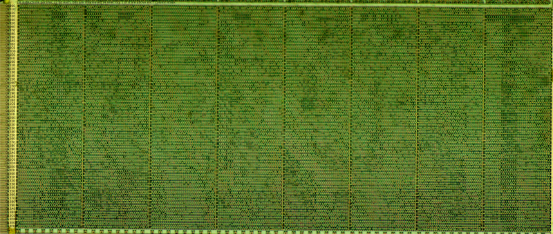
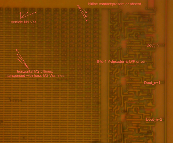
2 ROMs are present B1 and B6. Those ROMs use “drain contact programming”, for every data bit there is a N-fet transistor with Source connected to Vss, Gate connected to the wordline, but the drain may (logic 0) or may not (logic 1) be connected to the bitline.
When the 3 metal layers are removed (for example by etching), the connecting pads can be clearly seed and read. When the gold is present line is tied to ground and read as 0, when is missing (green spot), then line is read as 1. There are also 1:8 decoders, so to get valid data you need skip each 8 joints.
Identified fucntions in I-ROM
| addr | arguments | result | description |
|---|---|---|---|
| 0x20f9 | I2 = addr, D0 = 1 | B1 | read EEPROM (1B from 'addr' to B1) |
| 0x21d6 | I7 - addr?, D1 - uint16_t data | D1 ??? | store instruction memmory? |
| 0x21d9 | I7++ | D1 | load instruction memmory, (addr 0x2000 - 0x5FFF) |
| 0x22ac | I7, A0 ??? | ??? | used by stage 2 bootloader in latter stage of boot |
| 0x22af | I7, A0 ??? | ??? | used by stage 2 bootloader in latter stage of boot |
